GrainDrop v0.5: A Pocket Recorder, Designed Start to Finish
The idea came from wanting a pocket recorder that didn’t exist. Not a voice memo app on a phone. Not a dedicated field recorder with menus and levels and configuration. A single-purpose device: slide a switch, it records audio to a MicroSD card. Slide it back, it stops. No screen, no buttons, no setup.
I had spent years assembling electronics projects designed by other people. Kits, development boards, hobby modules that I wired together on perfboard. I never attempted my own PCB design. Not because I couldn’t learn the concepts, but because the tools had a reputation. KiCad. EDA software. The learning curve felt like a prerequisite course before the real work could start, and I could never justify that to myself.

GrainDrop v0.5 schematic — ESP32-S3-WROOM-1, INMP441 MEMS microphone, MicroSD slot, SPDT slide switch.
This time I brought Hermes along. I described what I wanted — pocket form factor, slide switch, always-on recording — and we started working through it together. The schematic came first. A Python script generated the KiCad sexpr format directly, producing the netlist and component positions. Then came the lessons. KiCad 10 requires UUIDs on every wire segment and junction. Wires must be drawn as single segments — no multi-point paths — and internal vertices need explicit junction elements. The Gerber export demands the board be positioned at the origin for JLCPCB to detect dimensions correctly. Mounting hole footprint pads need local origin coordinates, not absolute positions. Each of these cost time to discover, and none of them were hard once we knew them.

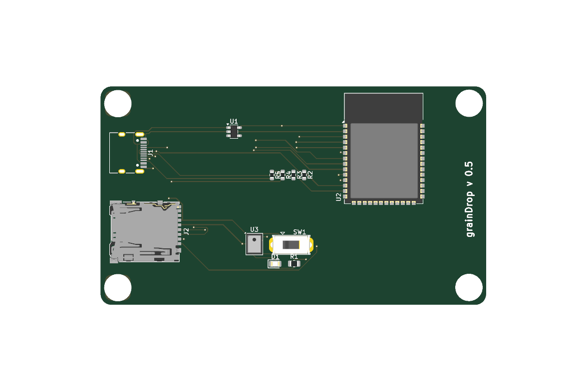
Final PCB layout: 90×51mm, two-layer, 37 nets, all traces routed. GND copper pour on bottom layer.
The breakthrough came when we found FreeRouting. KiCad’s built-in manual routing tools work, but routing a two-layer board with 37 nets by hand is tedious. The CLI workflow — export Specctra DSN from pcbnew, pipe it through the FreeRouting Java jar, import the resulting SES back — automated the routing in under three seconds. “Much better workflow,” I said after the first run. “Omg that was tedious to wire.” The difference between dreading a task and enjoying the iteration is often one tool discovery away, and that is exactly the kind of unlock I wanted from this project.
3D render of the assembled board. ESP32-S3 module, USB-C connector, INMP441 MEMS mic, MicroSD slot, slide switch, and indicator LED.
Postmortem. The board is JLCPCB-ready. Gerbers, BOM, and CPL files have been validated. The only component not available for assembly is the INMP441 MEMS microphone — out of stock at JLCPCB, which means either hand-soldering those or waiting for a restock. Total for five assembled boards: $207.40. For v0.6, I would shrink the footprint. The 90×51mm business-card shape was generous for the first iteration; a denser layout could fit in half the space. I also considered switching from the WROOM-1 module to the MINI-1 for a smaller profile, but the MINI-1 doesn’t break out USB OTG pins, and direct USB-C programming is worth keeping. The current design works. The next one will be tighter.
What I learned. I spent years telling myself PCB design was out of reach — that the tools were too complex, the knowledge gap too wide, the mistakes too expensive. The real bottleneck wasn’t KiCad. It was the absence of someone patient enough to work through the first board alongside me. AI didn’t design this board. I did. But I learned the tools faster because I had a collaborator who could catch the subtle format errors, explain the DSN/SES pipeline, and keep the iteration loop short enough that momentum never died. That is the only story worth telling here.